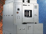
Nikon P3 Precision Pattern Profiler
Nikon Updated: 2007-06-20A new lithography inspection platform designed to improve product yield by capturing yield-limiting defects.
The Nikon P3 system is designed for automated pattern profile management and line width roughness monitoring of 300mm wafers with fully incorporated macro defect detection, EBR inspection, and automatic defect classification for unsurpassed performance down to the 55-nm node.
High Sensitivity
The P3 boasts high sensitivity to incremental changes in focus and exposure to provide stepper/scanner focus management, enabling partial SEM replacement.
Back-Side Inspection
The Nikon P3 integrated back-side inspection capability with real-time correlation to front-side defects ensures that the backside of the wafers will be free of defects prior to the photolithography process, ensuring that backside defects do not create an un-flat exposure surface leading to focus and exposure problems on the front-side of the wafer.
The back-side inspection capability ensures rapid detection of contamination such as surface particles, residues, scratches, contamination, or damage caused by equipment chucks and pallets to prevent them from being spread throughout the fab.
Automatic Defect Classification (ADC) and Auto-Rework Judgment
Automatic Defect Classification (ADC) and Auto-Rework Judgment allow users to specify their own rework criteria for each process. Adjusting the threshold of the defect criteria in the recipe provides automatic rework judgments in wafer and lot units.
Highlights
• Pattern Profile Management — Line Width Roughness and Line Edge Roughness monitoring using Nikon exclusive PER optics down to the 55-nm node for high level of sensitivity comparable to SEM
• Exclusive TLEX technology for Unsurpassed VIA/Hole process inspection
• Ready for 55-nm technology node
• Every wafer and entire surface inspection with high sensitivity to defocus errors to catch sudden litho cell problems
• High throughput of 180 wafers/hour, enabling 100% wafer and lot inspection
• Low false alarm rate
• Full host of web based analysis tools to help reduce manufacturing costs and time to market, ultimately leading to higher yields
There are no manuals currently available for this model.
Related Manuals
Nikon AMI-3000 Automatic Macro Inspection System
Nikon Optistation-3200 Wafer Inspection System
Nikon Optistation-3100 Wafer Inspection System
Nikon Optistation-7 Wafer Inspection System
Nikon Optistation-5 Wafer Inspection System
Nikon Eclipse 90i Advanced Automated Research Microscope System
Nikon Eclipse 80i Advanced Research Microscope
Nikon Eclipse FN1 Fixed Stage Microscope for Electrophysiological Research
Nikon Eclipse TE2000 Inverted Research Microscope Systems
Nikon Eclipse TE2000-PFS Inverted Research Microscope With Real-Time Focus Correction
Nikon NT88-V3 Micromanipulator Systems
Nikon Laser TIRF System
